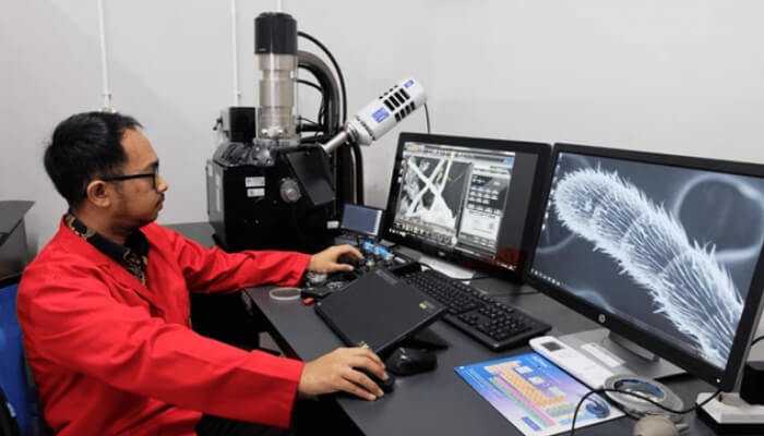
Particularly in recent years as the size of materials utilized in different applications continues to diminish, scanning electron microscopes (SEMs) have become potent and flexible instruments for material characterization.
Electron microscopes image using electrons in the same manner as light microscopes do. While SEMs employ the electrons reflected or knocked off the near-surface area of a sample to produce a picture, transmission electron microscopes (TEMs) detect electrons that travel through a very thin material. SEMs have better resolution than a light microscope since electron wavelengths are far less than those of light.
How SEMs work
The electron beam of scanning electron microscopy raster scans the material. The electron source generates first electrons at the top of the column. These are expelled when their thermal energy exceeds the work capability of the parent material. Then they are drawn to the positively charged anode and sped on.
The electron column as whole must be under vacuum. The electron source of an electron microscope is sealed within a unique chamber to maintain vacuum and guard against contamination, vibrations, and noise, just as with all parts of the instrument. Apart from guarding the electron source from contamination, vacuum lets the user obtain a high-resolution picture. Other atoms and molecules can find place in the column in the absence of vacuum. Their interactions with electrons cause the electron beam to deflect, therefore compromising the image clarity. Furthermore improving the electron collecting efficiency of the column-based detectors is high vacuum.
Controlling the path of electrons
Lenses are used to regulate electron path, much like in optical microscopes. The employed lenses are electromagnetic since electrons cannot travel through glass. They are just coils of wires housed within metal pole components. A magnetic field results from current passing through the coils. Since electrons are quite sensitive to magnetic fields, these electromagnetic lenses allow one to regulate their route inside the microscope column solely by changing the current given to them.
Two usually used forms of electromagnetic lenses are: First lens electrons encounter on their way to the sample is the condenser lens. Before the electron beam cone opens once more, this lens converges the beam; thereafter, the objective lens once more converges the beam. While the main purpose of the objective lens is to concentrate the electron beam onto the sample, the condenser lens specifies the size of the electron beam, hence defining the resolution.
Scanning coils found in the SEM’s lens system also help to raster the beam onto the material. Many times, apertures are coupled with lenses to vary the beam’s size.
Backscattered and secondary electrons
Many various kinds of electrons, photons, or irradiations can be produced by the interactions among the electrons in a sample. Regarding a SEM lab, secondary electrons (SE) and backscattered (BSE) electrons are the two forms of electrons employed for imaging.
Reflective back following elastic interactions between the beam and the sample, BSEs are members of the main electron beam. Conversely, secondary electrons come from the atoms of the sample; inelastic interactions between the electron beam and the sample produce them.
Different kinds of signals a SEM uses and their source area.
BSEs originate from deeper parts of the sample and SEs come from surface areas, hence the two provide distinct kinds of information. High sensitivity to atomic number BSE scans demonstrate; the material appears brighter in the image the higher its atomic number. More finely defined surface information is available from SE imaging.
Elemental analysis of the sample is also extensively employed in many microscopes using detection of X-rays produced from the electron-matter interaction. Every substance generates X-rays with a designated energy; these constitute the fingerprint of the material. One can determine all the many elements in a sample by spotting the energies of X-rays emanating from an unknown composition.
How electrons are detected
Different kinds of detectors help to detect BSEs and SEs. To maximize BSE collecting, solid state detectors are positioned above the sample, concentrically to the electron beam.
Mostly utilized for SE detection is the Everhart-Thornley detector. It comprises a Faraday cage’s positively charged scintillator within which the SEs are attracted. Before reaching a photomultiplier for amplification, the electrons are accelerated and turned into light using the scintillator.
To maximize the efficiency of spotting SEs—which are then utilized to create a 3D-image of the material displayed on a PC monitor—the SE detector is positioned at an angle at the side of the electron.
SEM: Magic But Meticulous
As you can see, before an image appears on your monitor, the electrons have to pass several steps. Naturally, you do not have to wait for the electrons to complete their trip; the entire process occurs practically instantly within nanoseconds. To get a high-quality image at the same time, every “step” of an electron inside the column must be pre-calculated and under control with exactness.


